


12V TO 24V @ 1A STEP-UP SWITCHING REGULATOR USING LM2585
This is a DC-DC step-up converter based on LM2585-ADJ regulator manufactured by Texas Instruments. This IC was chosen for its simplicity of use, requiring minimal external components and for its ability to control the output voltage by defining the feedback resistors (R1,R2). NPN switching/power transistor is integrated inside the regulator and is able to withstand 3A maximum current and 65V maximum voltage. The switching frequency is defined by the internal oscillator and it’s fixed at 100KHz.
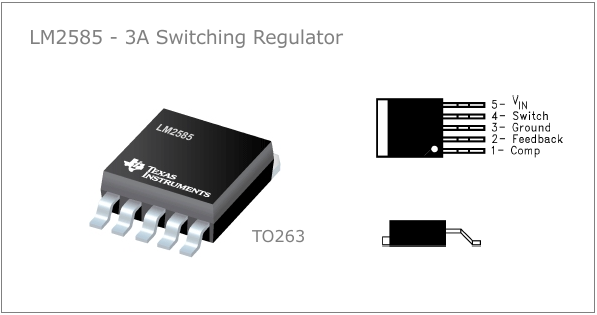
The power switch is a 3-A NPN device that can standoff 65 V. Protecting the power switch are current and thermal limiting circuits and an under-voltage lockout circuit. This IC contains a 100-kHz fixed-frequency internal oscillator that permits the use of small magnetics. Other features include soft start mode to reduce in-rush current during start-up, current mode control for improved rejection of input voltage, and output load transients and cycle-by-cycle current limiting. An output voltage tolerance of ±4%, within specified input voltages and output load conditions, is specified for the power supply system.
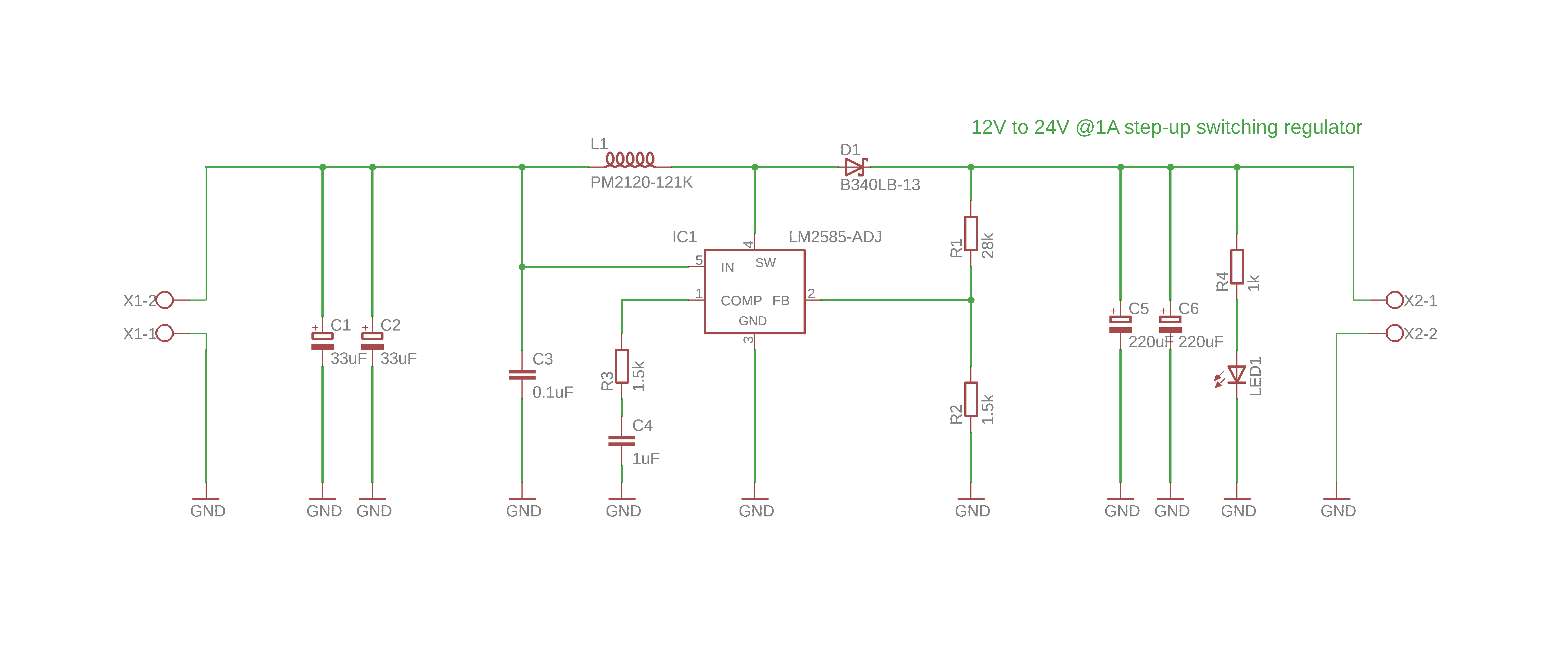
Schematic
SPECIFICATIONS
- Vin: 10-15V DC
- Vout: 24V DC
- Iout: 1A
- Frequency: 100KHz
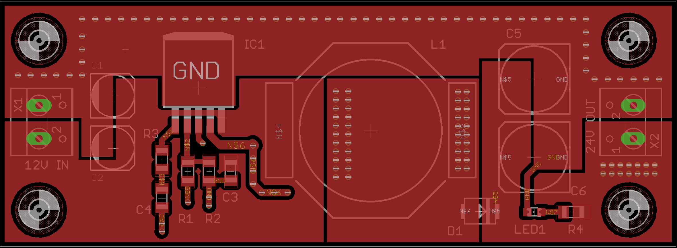
Schematic is a simple boost topology arrangement based on datasheet. Input capacitors and diode should be placed close enough to the regulator to minimize the inductance effects of PCB traces. IC1, L1, D1, C1,C2 and C5,C6 are the main parts used in voltage conversion. Capacitor C3 is a high-frequency bypass capacitor and should be placed as close to IC1 as possible.
All components are selected for their low loss characteristics. So capacitors selected have low ESR and inductor selected has low DC resistance.
At maximum output power, there is significant heat produced by IC1 and for that reason, we mounted it directly on the ground plane to achieve maximum heat dissipation.
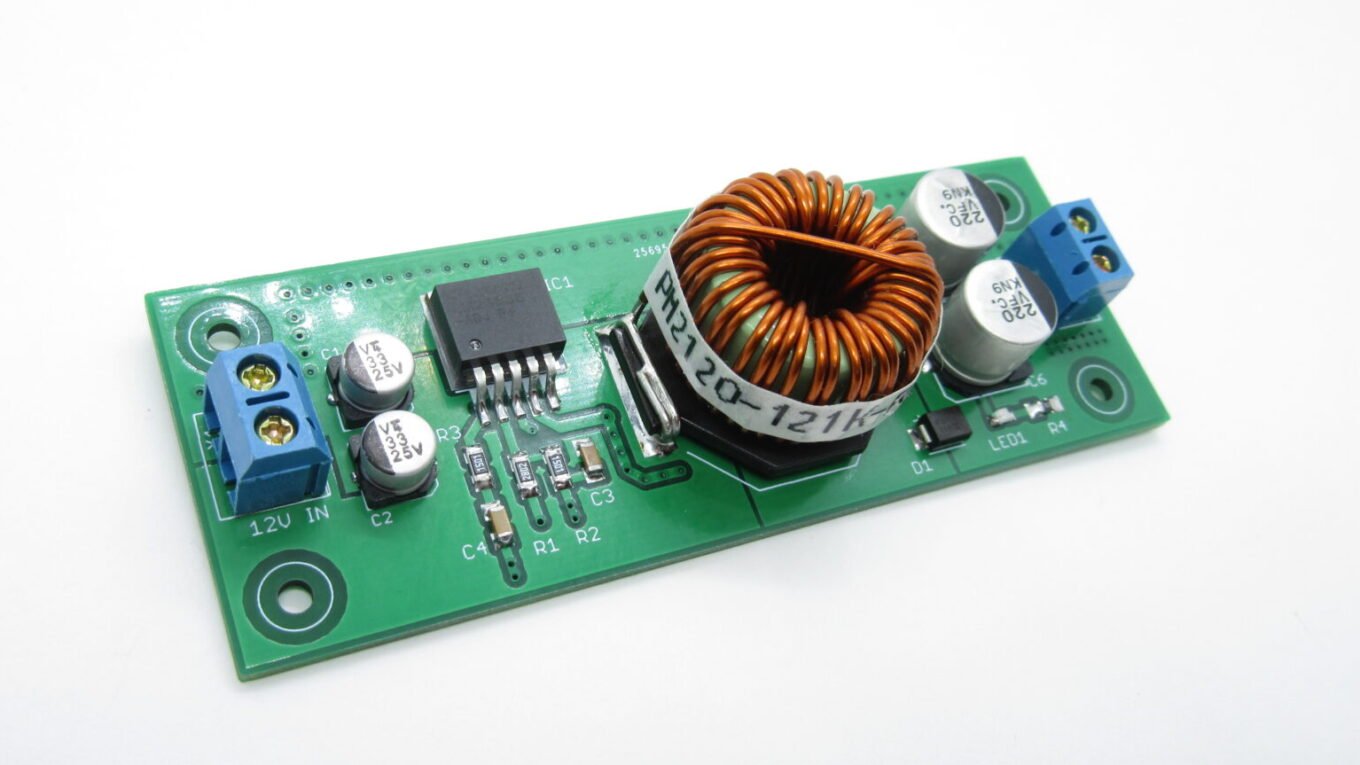
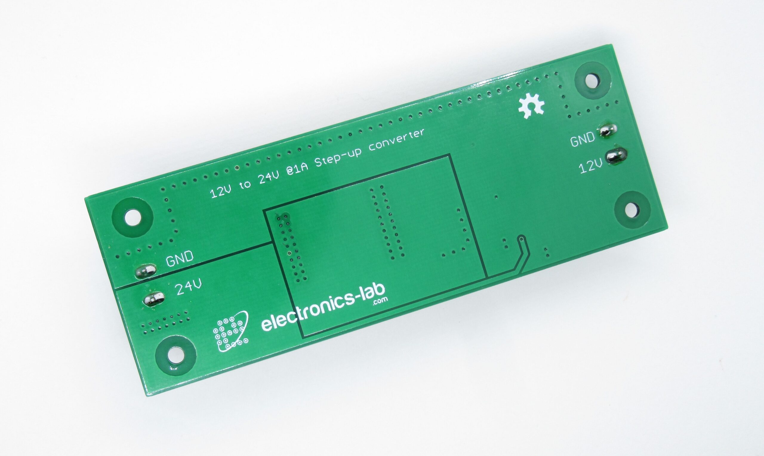
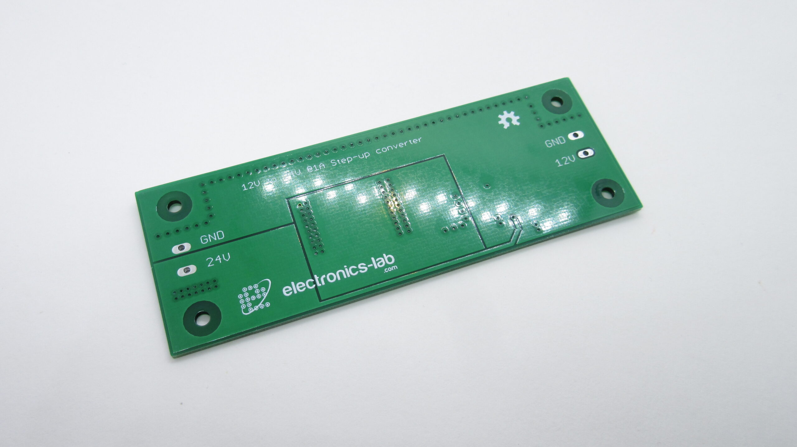
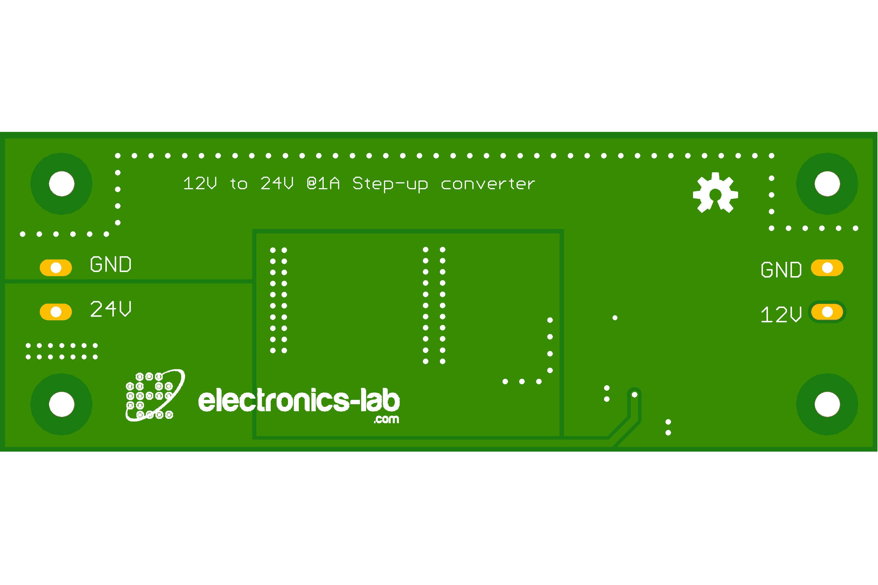
PHOTOS

PARTS LIST
| Part | Value | Package | MPN | Mouser No |
|---|---|---|---|---|
| C1 C2 | 33uF 25V 1Ω | 6.3 x 5.4mm | UWX1E330MCL1GB | 647-UWX1E330MCL1 |
| C3 | 0.1uF 50V 0Ω | 1206 | C1206C104J5RACTU | 80-C1206C104J5R |
| C4 | 1uF 25V | 1206 | C1206C105K3RACTU | 80-C1206C105K3R |
| C5 C6 | 220uF 35V 0.15Ω | 10 x 10.2mm | EEE-FC1V221P | 667-EEE-FC1V221P |
| D1 | 0.45 V 3A 40V Schottky | SMB | B340LB-13-F | 621-B340LB-F |
| IC1 | LM2585S-ADJ | TO-263 | LM2585S-ADJ/NOPB | 926-LM2585S-ADJ/NOPB |
| L1 | 120 uH 0.04Ω | 30.5 x 25.4 x 22.1 mm | PM2120-121K-RC | 542-PM2120-121K-RC |
| R1 | 28 KΩ | 1206 | ERJ-8ENF2802V | 667-ERJ-8ENF2802V |
| R2 R3 | 1.5 KΩ | 1206 | ERJ-8ENF1501V | 667-ERJ-8ENF1501V |
| R4 | 1 KΩ | 1206 | RT1206FRE07931KL | 603-RT1206FRE07931KL |
| LED1 | RED LED 20mA 2.1V | 0805 | 599-0120-007F | 645-599-0120-007F |
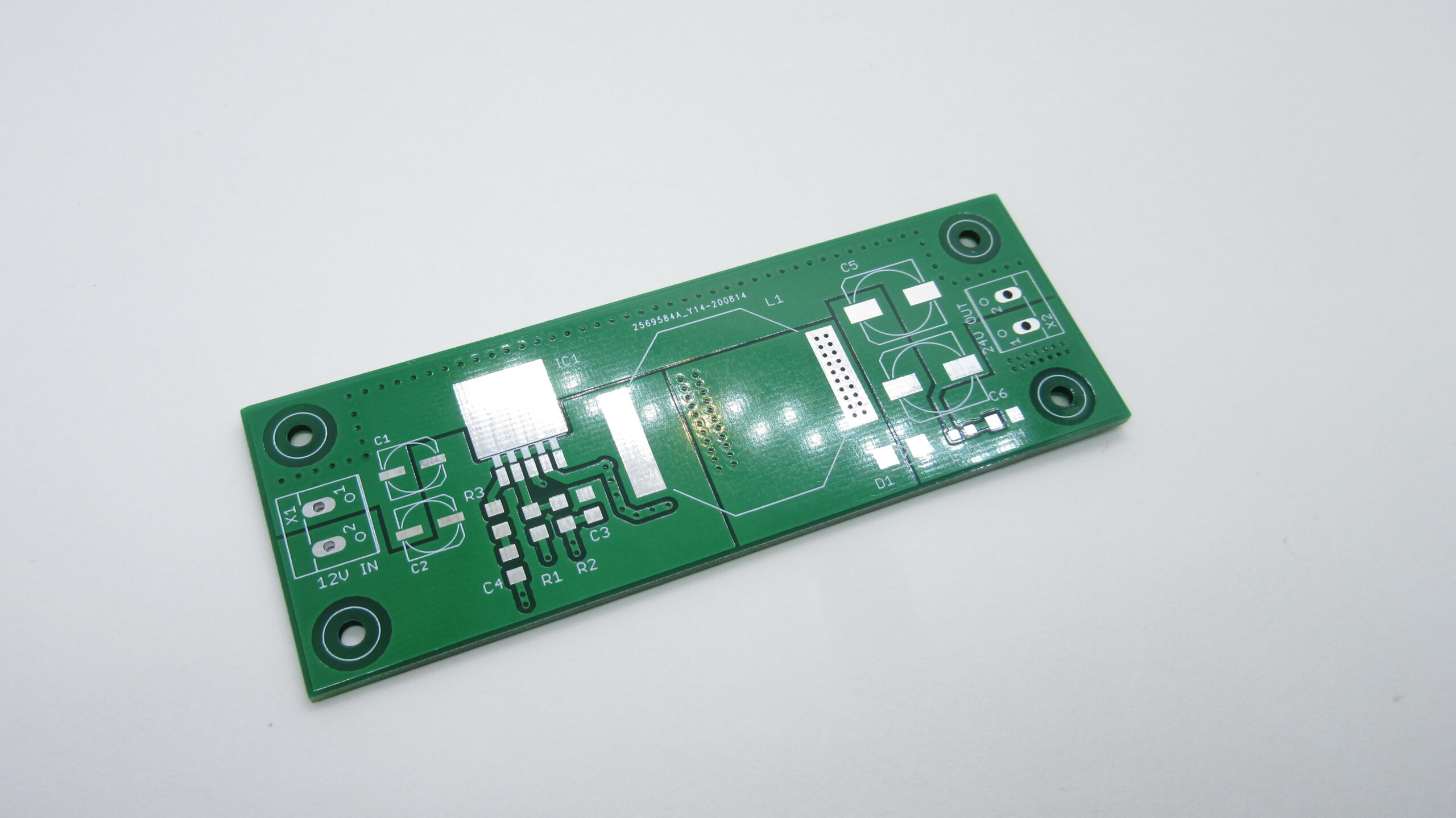
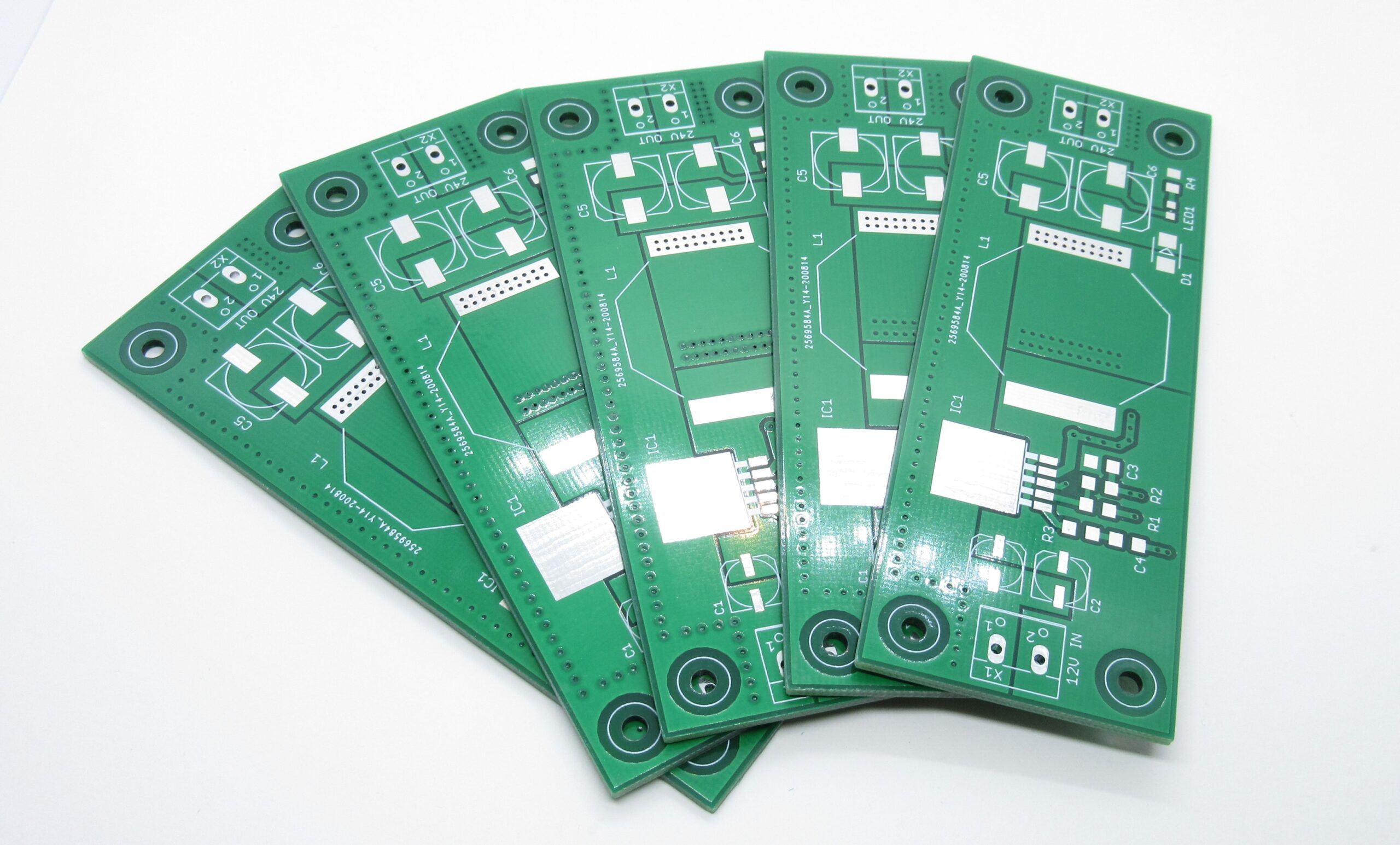
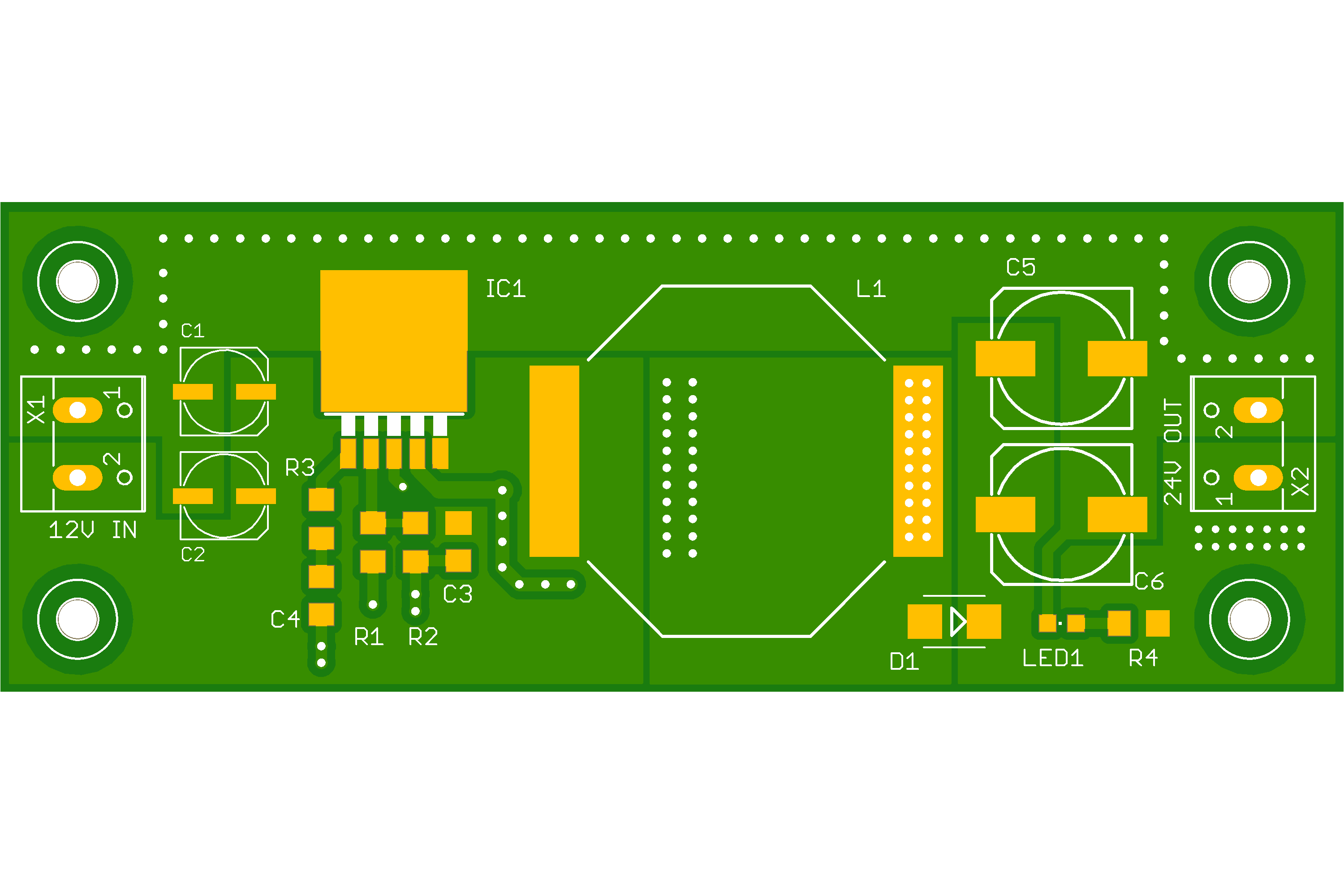
GERBER VIEW
SIMULATION
We’ve done a simulation of the LM2585 step-up DC-DC converter using the TI’s WEBENCH online software tools and some of the results are presented here.
The first graph is the open-loop BODE graph. In this graph, we see a plot of GAIN vs FREQUENCY in the range 1Hz – 1M and PHASE vs FREQUENCY in the same range. This plot is useful as it gives us a detailed view of the stability of the loop and thus the stability and performance of our DC-DC converter.
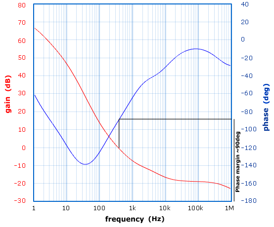
What’s interesting on this plot is the “phase margin” and “gain margin“. The gain margin is the gain for -180deg phase shift and phase margin is the phase difference from 180deg for 0db gain as shown in the plot above. For the system to be considered stable there should be enough phase margin (>30deg) for 0db gain or when phase is -180deg the gain should be less than 0db.
On the plot above we see that the phase margin is ~90deg and that ensures that the DC-DC converter will be stable over the measured range.
The next simulation graph is the Input Transient plot over time.
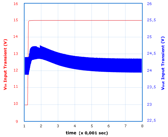
In this plot, we see how the output voltage is recovering when the input voltage is stepped from 10V to 15V. We see that 4ms after the input voltage is stepped the output has recovered to the normal output voltage of 24V.
The next graph is the Load Transient.
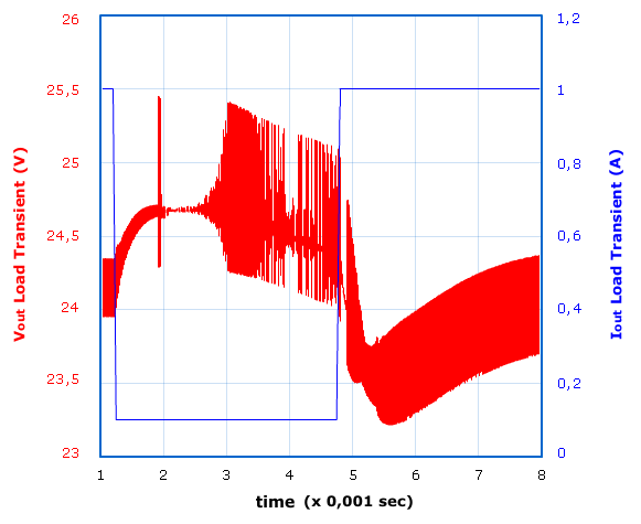
Load Transient simulation
Load transient is the response of output voltage to sudden changes of load or Iout. We see that the output current suddenly changes from 0,1A to 1A and that the output voltage drops down to 23,2V until it recovers in about 3ms. We also see that when the load is reduced from 1A to 0,1A, output voltage spikes up to ~25,5V, then rings until it recovers to 24V in about 4ms.
The last graph shows the Steady State operation of DC-DC converter @ 1A output.
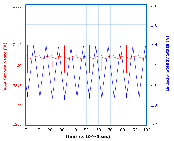
This graph shows the simulated output voltage ripple and inductor current. We see that output voltage ripple is ~0,6Vpp and the inductor current has a peak current of 2,4A. The inductor we used is rated at max 5,6A DC so it can easily withstand such operating current and without much heating of the coil.
Operating point data (Vin=13V, Iout=1A)
| Operating Values | |||
| Pulse Width Modulation (PWM) frequency | Frequency | 100 kHz | |
| Continuous or Discontinuous Conduction mode | Mode | Cont | |
| Total Output Power | Pout | 24.0 W | |
| Vin operating point | Vin Op | 13.00 V | |
| Iout operating point | Iout Op | 1.00 A | |
| Operating Point at Vin= 13.00 V,1.00 A | |||
| Bode Plot Crossover Frequency, indication of bandwidth of supply | Cross Freq | 819 Hz | |
| Steady State PWM Duty Cycle, range limits from 0 to 100 | Duty Cycle | 48.3 % | |
| Steady State Efficiency | Efficiency | 93.2 % | |
| IC Junction Temperature | IC Tj | 65.2 °C | |
| IC Junction to Ambient Thermal Resistance | IC ThetaJA | 34.9 °C/W | |
| Current Analysis | |||
| Input Capacitor RMS ripple current | Cin IRMS | 0.14 A | |
| Output Capacitor RMS ripple current | Cout IRMS | 0.48 A | |
| Peak Current in IC for Steady State Operating Point | IC Ipk | 2.2 A | |
| ICs Maximum rated peak current | IC Ipk Max | 3.0 A | |
| Average input current | Iin Avg | 2.0 A | |
| Inductor ripple current, peak-to-peak value | L Ipp | 0.50 A | |
| Power Dissipation Analysis | |||
| Input Capacitor Power Dissipation | Cin Pd | 0.01 W | |
| Output Capacitor Power Dissipation | Cout Pd | 0.035 W | |
| Diode Power Dissipation | Diode Pd | 0.45 W | |
| IC Power Dissipation | IC Pd | 1.0 W | |
| Inductor Power Dissipation | L Pd | 0.16 W | |
CONFIGURING OUTPUT VOLTAGE
The output voltage is configured by R1, R2 according to the following expression (Vref=1,23V)
VOUT = VREF (1 + R1/R2)
If R2 has a value between 1k and 5k we can use this expression to calculate R1:
R1 = R2 (VOUT/VREF − 1)
For better thermal response and stability it is suggested to use 1% metal film resistors.
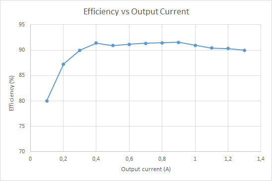
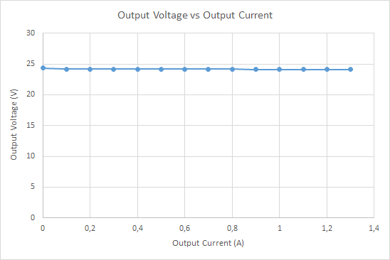
MEASUREMENTS
LM2585-ADJ DATASHEET
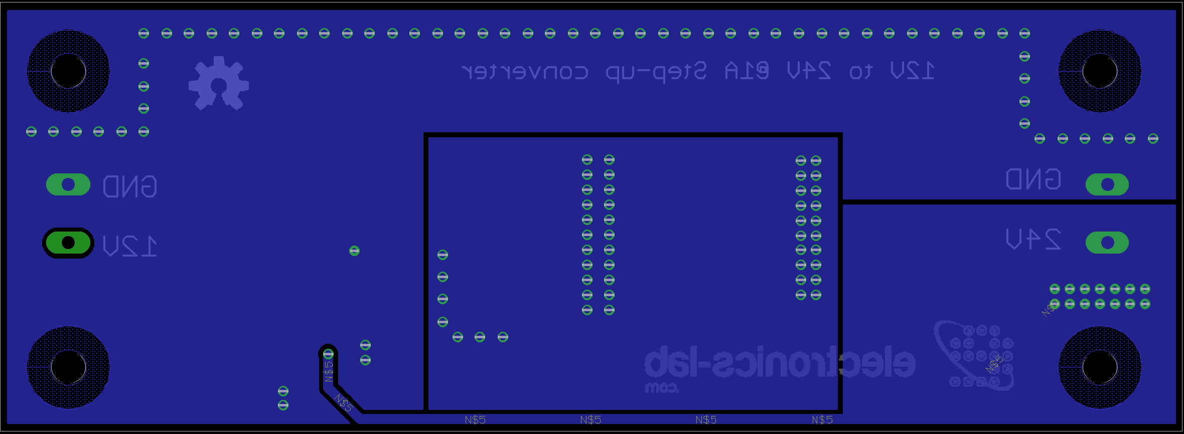
PCB
🛠️ Dive into our collection of DIY Kits, 🔊 Audio Amplifiers, Digital Scoreboards, FM transmitters, and more!
🎶 Explore endless possibilities at our new store.