


Blog
Recent Posts
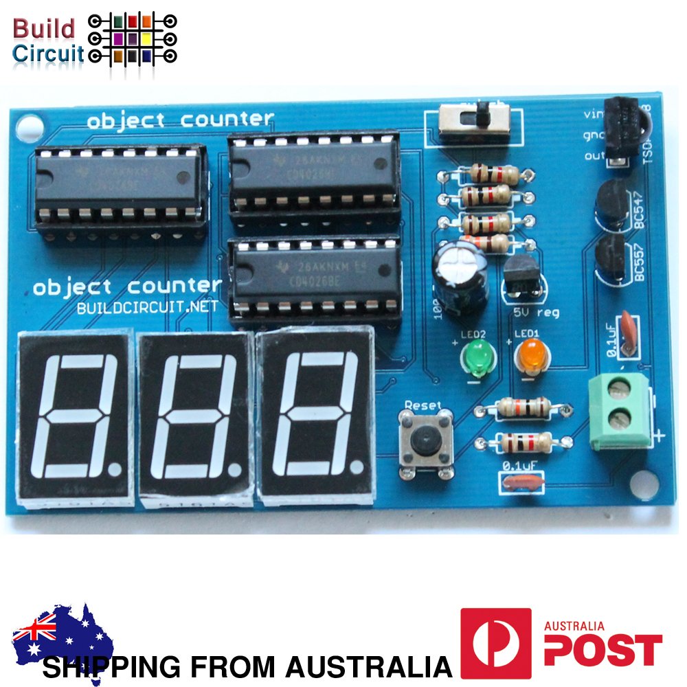
Arduino Projects

Basic Introduction to NextDFM software

10 Tips to choose a Prototype PCB Assembly Manufacturer
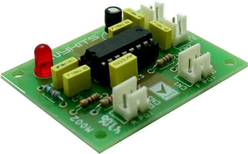
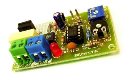
CONTACTLESS AUTOMATIC WARDROBE LED LIGHT WITH FADE EFFECT
LUX METER MODULE
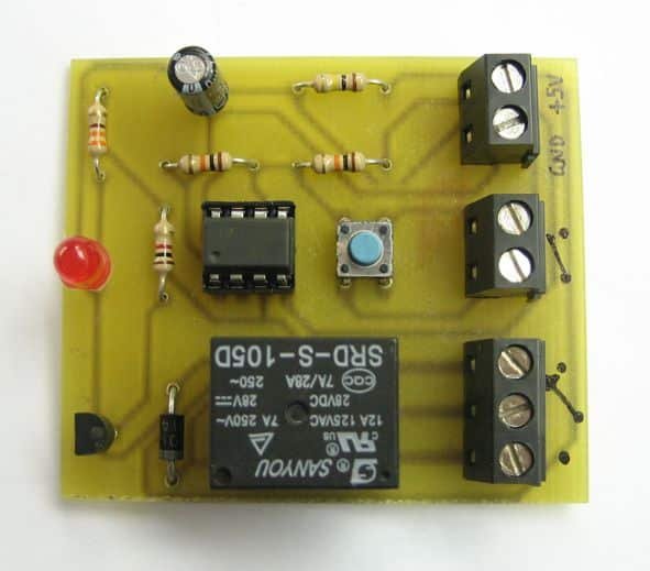
SOUND ACTIVATED SWITCH – RELAY
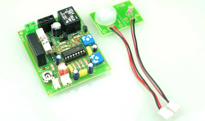
PIR SENSOR
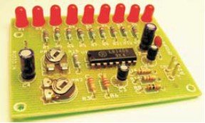
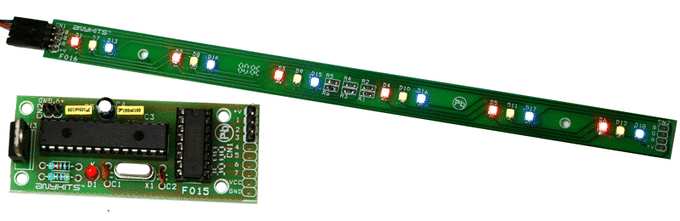
AUDIO VU METER 9 LEDS
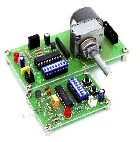
IR REMOTE VOLUME CONTROLLER
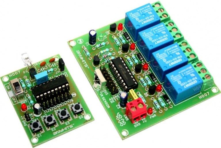
4 CHANNEL INFRARED REMOTE RELAYS
TOGGLE ON / OFF SWITCH
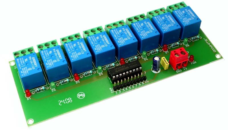
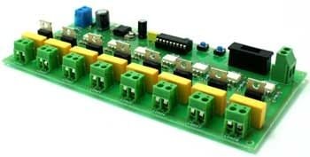
8 CHANNEL RELAY BOARD
ELECTRONIC TOGGLE SWITCH
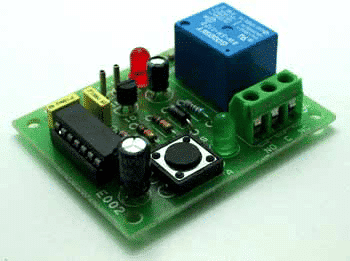
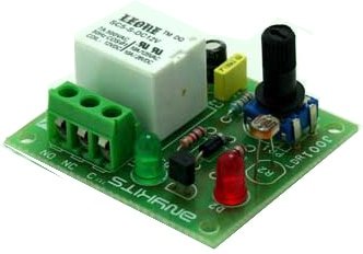
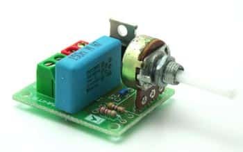
ONE CHANNEL RELAY DRIVER

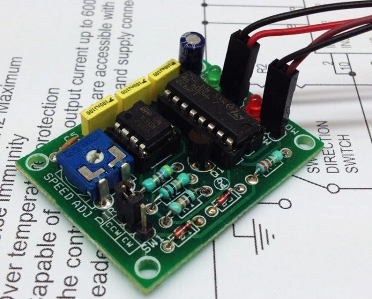
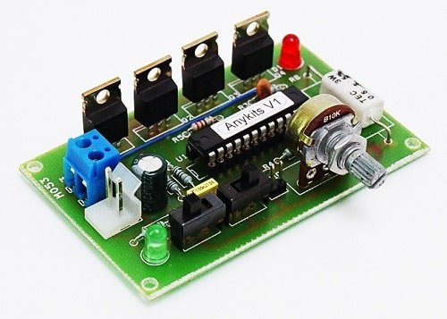
DC MOTOR DIRECTION CONTROLLER WITH TACT SWITCHES
DC SERVO MOTOR DRIVER
UNIPOLAR 4-PHASE STEPPER MOTOR CONTROLLER

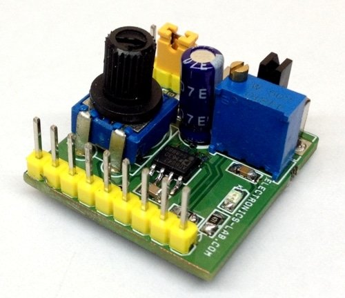
RC SERVO DRIVER 0-5V

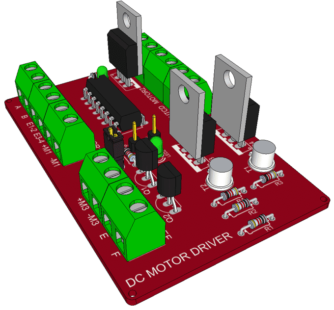
L293D DC MOTOR DRIVER MODULE
DC MOTOR SPEED AND DIRECTION CONTROLLER USING L293D

HALF BRIDGE DRIVER BASED ON IR2104

AC MOTOR SPEED CONTROLLER USING U2008B

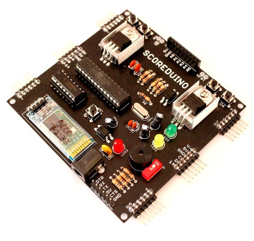
Scoreduino-B Arduino based controller for digital scoreboards

Single digit common anode up and down counters/drivers for seven segments displays
PULSE GENERATOR FOR STEPPER CONTROLLER USING AD654

Scoreduino-A Trigger Module For Up and Down Counter Drivers

Basic trigger module for up down counters

Single digit up and down counter using 74LS192 and RF remote control
Scoreduino
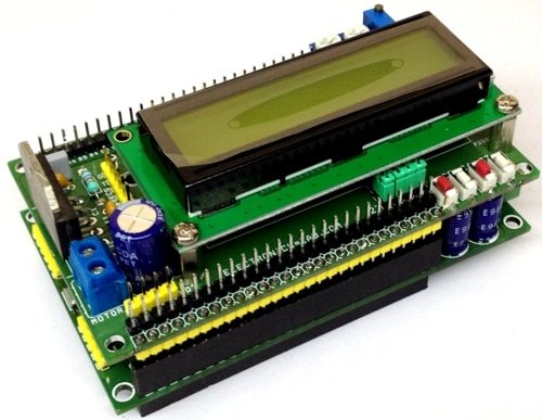
16X2 LCD SHIELD WITH LMD18201 MOTOR DRIVER
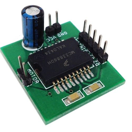
DC MOTOR & DIRECTION CONTROLLER WITH BRAKE USING MC33035

Make a seven segment display using 5mm LEDs
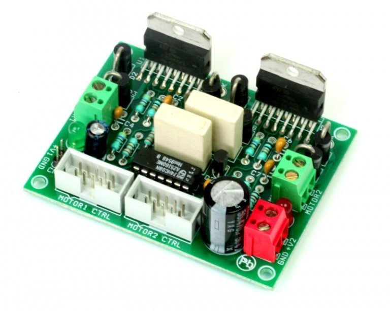
2X L298 DUAL DC MOTOR DRIVER BOARD FOR ROBOTS
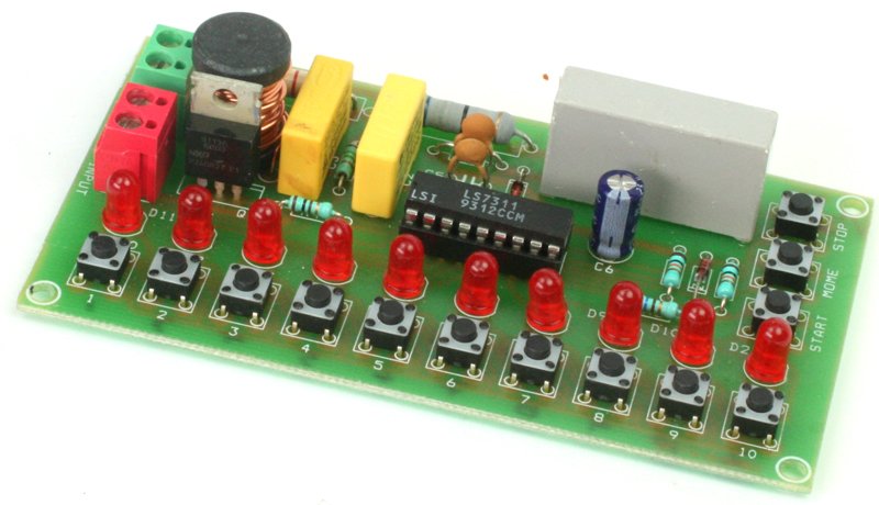
AC MOTOR SPEED CONTROLLER FOR MODERN APPLIANCES USING LS7311
2.5A 2 PHASE MICRO-STEPPING STEPPER MOTOR DRIVER

50V – 10A BIDIRECTIONAL DC MOTOR DRIVER USING A3941
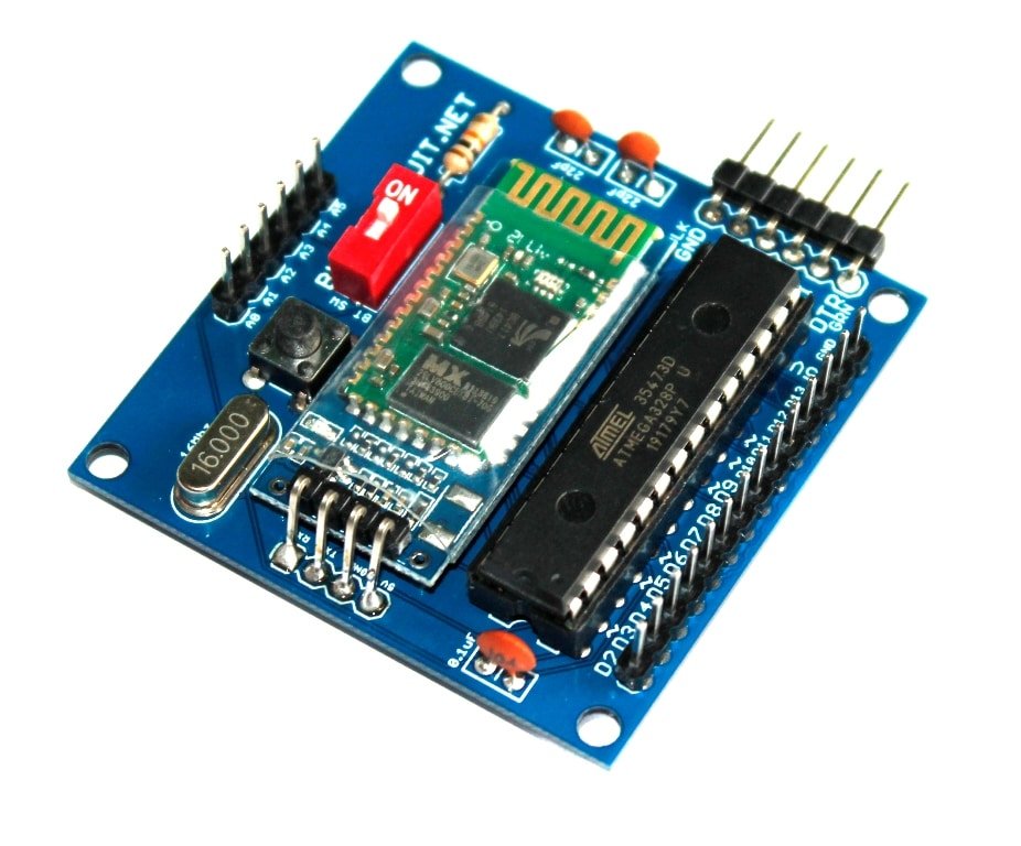
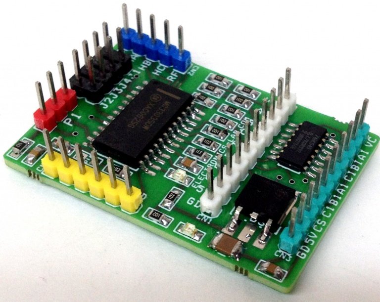
Popular Android Apps for 12CH Bluetooth Arduino module
3.5A UNIPOLAR STEPPER MOTOR DRIVER
MC33035 BRUSHLESS MOTOR DRIVER BREAKOUT BOARD

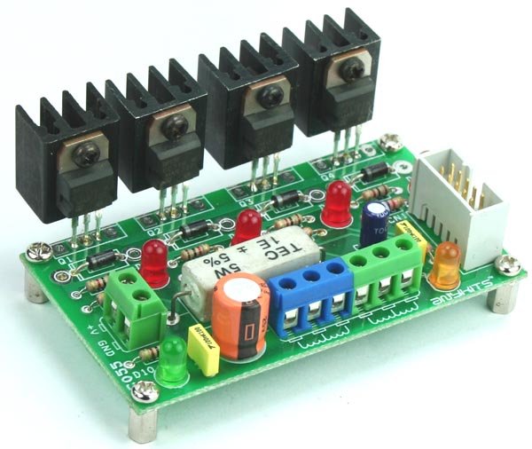
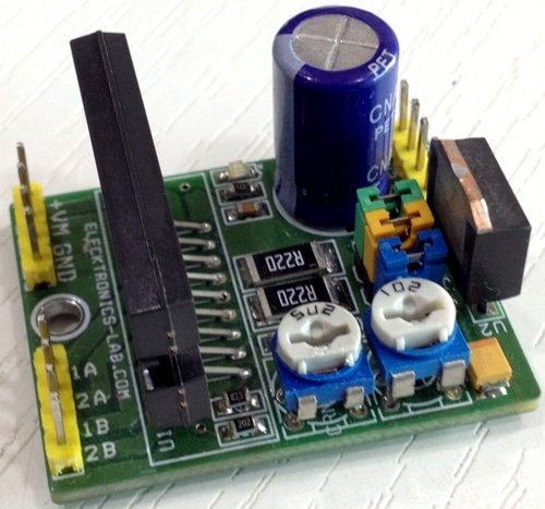
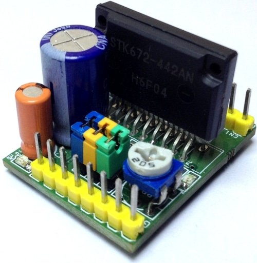
4A PWM CONTROLLED UNIPOLAR STEPPER MOTOR DRIVER USING STK672-740
15A 100V ISOLATED HALF-BRIDGE DRIVER

3V TO 5V BOOST DC-DC CONVERTER USING MAX711
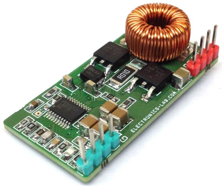
50V TO 5V @7A SYNCHRONOUS BUCK (STEP-DOWN) CONVERTER
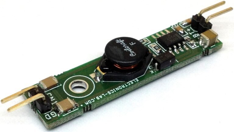
SINGLE 18650 LIPO BATTERY TO 5V BOOST CONVERTER
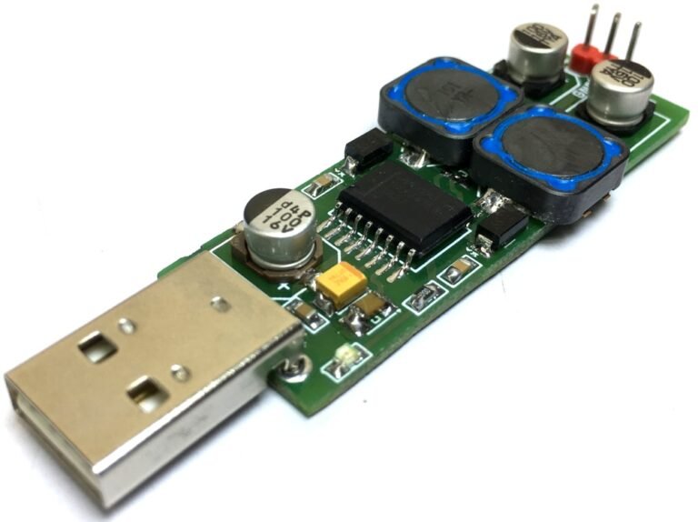
USB (5V) TO DUAL OUTPUT +/-15V OR +/-12V STEP-UP DC-DC CONVERTER
200W LAMP FLASHER
555 STEPPER PULSE GENERATOR
10 factors that affect the transmission range of DIY FM Transmitters
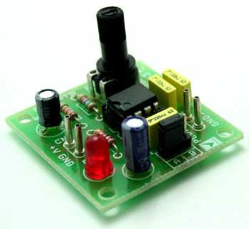
DARK SENSITIVE SWITCH
DC MOTOR DRIVER USING L293D
TRIAC BASED LAMP DIMMER
MICROCONTROLLER BASED RUNNING LIGHT CONTROLLER
RGB LED DISCO LIGHTS
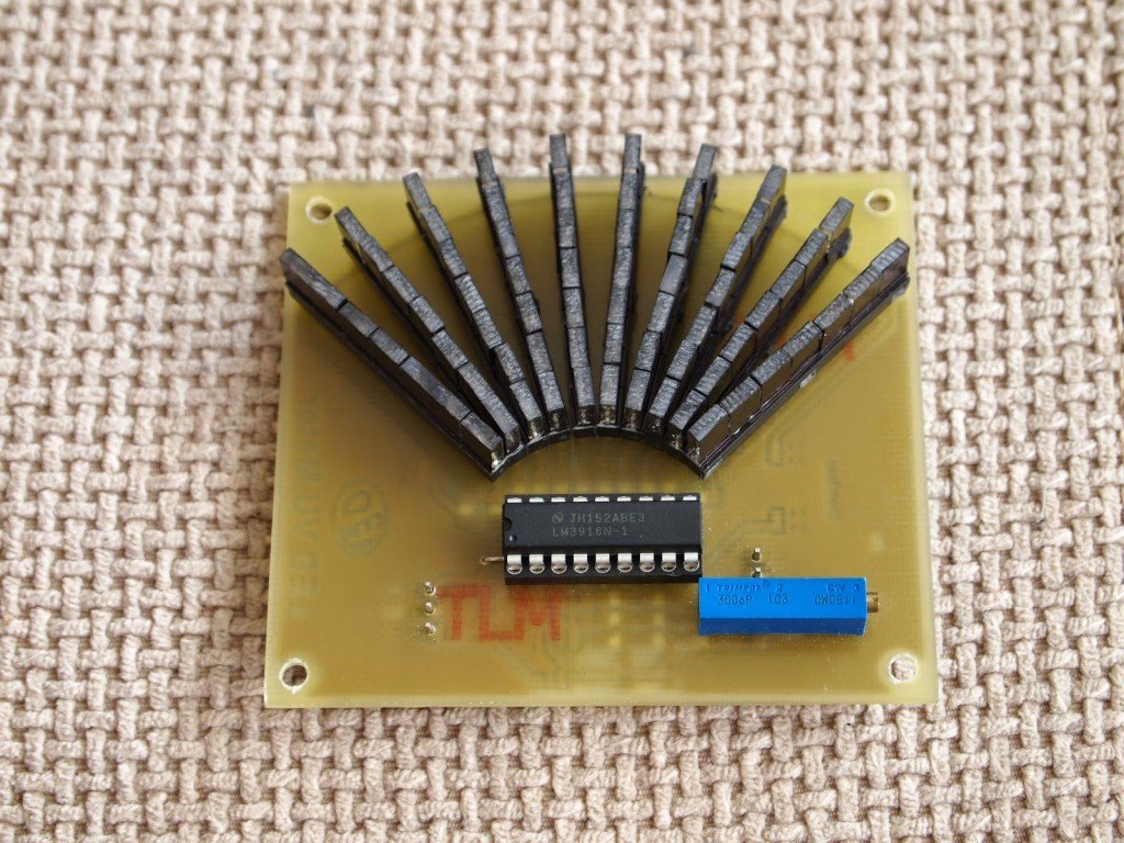
LED VU METER WITH LM3916
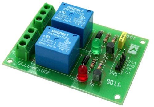
2 CHANNEL RELAY BOARD
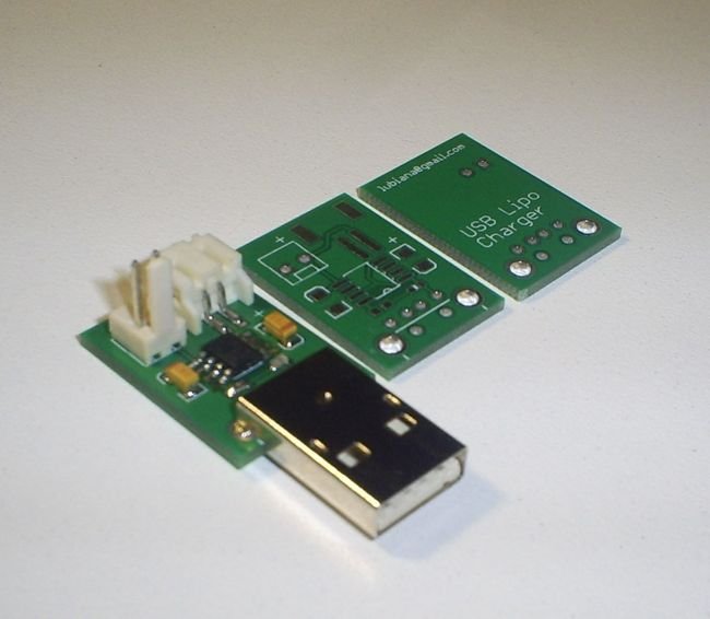
USB SINGLE CELL LIPOLY CHARGER

LASER DIODE DRIVER

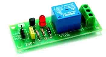
SINGLE CHANNEL SMD RELAY DRIVER
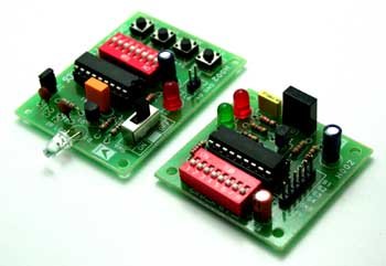
4 CHANNEL INFRARED REMOTE MODULE
5 AMP H-BRIDGE DC MOTOR DRIVER USING MC33886
November 13, 2020