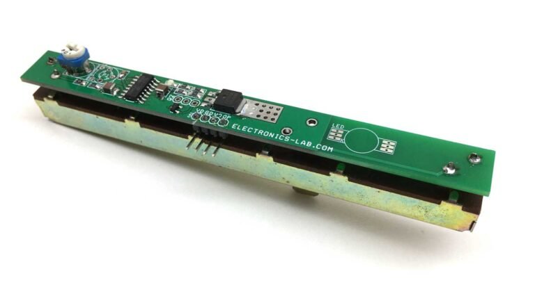
SIMPLE PRESSURE SENSOR AMPLIFIER & OVER PRESSURE SWITCH

The pressure sensor amplifier built using LM358 op-amp and MPXM2051GS pressure sensor from NXP semiconductor.  The circuit provides 4V output for full scale pressure input 0-7.5PSI.  One op-amp is used as amplifier and 2nd op-amp is used as comparator to provide an output at set value that can be used as over pressure switch to control a pump or solenoid.  This is a low cost general-purpose circuit for those applications where +/-3% performance is acceptable. Multi turn potentiometers are provided for Offset, span adjust & over/under Pressure set point to control output devices like solid state relay, Pump, and solenoid.

Features

  • Supply 12V DC
  • Pressure Sensor range 0-7.5PSI
  • Output 0-4V (Approx.)
  • PR1 Multi-Turn Potentiometer Offset
  • PR2 Multi-Turn Potentiometer Span Set
  • PR3 Multi-Turn Potentiometer Comparator (Switch) output Set
  • D1 Power LED
  • CN1 4 Header Connector Outputs & Supply Input

SCHEMATIC

PARTS LIST

CONNECTIONS

PCB

CURRENT SENSOR AMPLIFIER & OVER CURRENT SWITCH

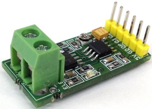
Current sensor amplifier and over current switch project is based on ACS714-30A current sensor and LM358 Op-amp, ½ of LM358 op-amp used as an amplifier for low voltage  and 2nd 1/2 LM358 op-amp used as comparator which provides over current TTL output, trimmer potentiometer provided to set the over current limit.  ACS714 sensor measures the current up to +/-30Amps, final output of the amplifier is 235mV/1A, and normally over current output is High-TTL, its goes low once the current over shoot than a set point. Circuit requires 5V DC and 40mA, Onboard LED indicates the power. Resistor divider R1, R3 provides bus voltage output for micro-controller interface to measure the bus voltage, choose appropriate value for R3, R1 as per your application and bus voltage, it’s should be less than 5V DC.

ACS714 Current Sensor

The Allegro™ ACS714 provides economical and precise solutions for AC or DC current sensing in automotive systems. The device package allows for easy implementation by the customer. Typical applications include motor control, load detection and management, switch-mode power supplies, and overcurrent fault protection. The device consists of a precise, low-offset, linear Hall circuit with a copper conduction path located near the surface of the die. Applied current flowing through this copper conduction path generates a magnetic field which the Hall IC converts into a proportional voltage. Device accuracy is optimized through the close proximity of the magnetic signal to the Hall transducer. A precise, proportional voltage is provided by the low-offset, chopper-stabilized BiCMOS Hall IC, which is programmed for accuracy after packaging. The output of the device has a positive slope (>VIOUT(Q)) when an increasing current flows through the primary copper conduction path (from pins 1 and 2, to pins 3 and 4), which is the path used for current sampling. The internal resistance of this conductive path is 1.2 mΩ typical, providing low power loss. The thickness of the copper conductor allows survival of  the device at up to 5× overcurrent conditions.

FEATURES

  • Supply 5V DC
  • ACS714-30 low noise direct output 66mV/Amp
  • LM358 Amplifier Output 235mV/Amp
  • Over Current Output (Normally High-TTL Goes low at over current set point)
  • Trimmer Preset to set the Over current limit
  • Bus voltage output
  • Power LED
  • Screw Terminal for Current
  • Header Connector for outputs and supply

HEADER CONNECTOR CONNECTIONS

  • Pin 1 :  VCC 5V DC Supply
  • Pin 2 : Supply GND
  • Pin 3 : VOP- ACS715-30 Sensor Direct Output 66mV/Amp
  • Pin 4 : OP1- Amplifier Output 235mV/amp
  • Pin 5 : OP2 Over Current  Output ( Normally High-TTL, Goes Low at Over Limit)
  • Pin 6 : BSV- Bus Voltage Output

SCHEMATIC

PARTS LIST

CONNECTIONS

PCB PHOTO

PCB

ISOLATED GATE MOSFET DRIVER BASED DC MOTOR AND SOLENOID DRIVER ARDUINO NANO SHILED

This is an Isolated gate driver-based N channel Mosfet Arduino Nano shield based on Si8261ACC, which can be used in various applications like DC Motor driver, solenoid driver, led driver, bulb driver and heater driver, with 3A fast switching diode provided across the output for an inductive load which protects the circuit from back EMF. Arduino Nano can be used to generate on/off signal or PWM for speed control. The board can also be used as a standalone driver by feeding 3-5V directly to the LED of the Si8261ACC gate driver. MOSFET can handle up to load 3A and DC supply at 12-24V DC. PWM Pin D3 of Arduino connected to gate driver IC.

FEATURES

  • Supply 12-24V DC
  • Load Up To 3Amps
  • Arduino Nano D3-PWM Pin connected to gate driver
  • PCB Dimensions 38.47mm X 17.46mm

SCHEMATIC

PARTS LIST

CONNECTIONS

PHOTOS

PCB

DC OUTPUT SOLID STATE RELAY

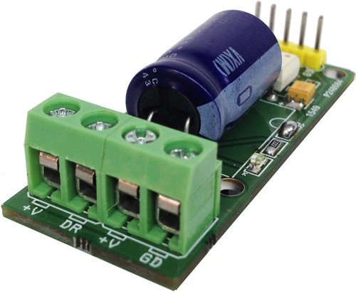
DC Output Solid State Relay 10Amps 60V DC (Optically Isolated Input)

This project has been designed around TLP250/352 which is Opto-Coupler IGBT/MOSFET Gate Driver from Toshiba and Mosfet IRFP260 from IR, This relay consists of optically isolated gate driver and low impedance Mosfet. The combination of low resistance and high load current handling capabilities make this Relay suitable for a variety of switching applications.  These devices are ideally suited for controlling high voltage and current DC loads with solid state reliability while providing 3750V isolation from input to output.

A solid-state relay (SSR) is an electronic switching device that switches on or off when a small external voltage is applied across its control terminals. SSRs consist of a Opto-isolator  which responds to an appropriate input (control signal), a solid-state electronic switching device which switches power to the load circuitry, and a coupling mechanism to enable the control signal to activate this switch without mechanical parts. This relay designed to switch DC Load up to 10Amps. It serves the same function as an electromechanical relay, but has no moving parts. Solid-state relays have fast switching speeds compared with electromechanical relays, and have no physical contacts to wear out. Input trigger voltage 3V to 9V DC (1.5V to 12 V with Transistor) and output load 10Amps and supply 12V to 60V DC (100V DC also Possible). Gate Driver required supply 12V to 18V DC. Heat sink required for peak load.

  • NOTE 1: Q2, R1, J2 Are Optional for Low Current Trigger Signal Input
  • NOTE 2: J1 (VC-J) Close In Case of Load Supply and Logic Gate Supply are same 12V to 18V DC for single supply input operation
  • NOTE 3: Done use R4, D1 LED If Load Supply is higher than 24V DC
  • NOTE 4: J3 for Cathode ground in case of single pulse input

FEATURES

  • +V Supply 60V DC (100V DC Possible) For Load
  • VC Supply 12V – 18V DC for Opto-Coupler Gate Driver
  • J1 Jumper for Single Supply operations ( If the Load Supply is between 12V DC to 18V DC)
  • Load Current Up to 10Amps (Required large size Heat sink for High current Load)
  • Two Input Options: 1. Anode Cathode Input 2. Signal input through Transistor Base input
  • Input Trigger 3V to 9V DC-Anode and Cathode ( Alter Resistor Value for 24V DC Trigger Input )
  • Signal Input 1.5V to 12V DC at Transistor Base ( Alter Base Resister Value for Higher trigger input)
  • Isolation Voltage : 3750V ( Gate Driver)
  • Operation Input Frequency up to 50Khz ( Refer TLP352 Data Sheet for More info)

CONNECTIONS

  1. Cathode 2. Anode 3. Low Current Signal in 4. VCC-12V-18V 5. GD-Ground
  2. +V & GD Load Supply 12V to 60V DC
  3. +V & DR Load ( DR-Drain: –Load & +V: + Load)

APPLICATIONS

  • Motor Controls
  • Robotics
  • Medical Equipment
  • Railroad/Traffic Controls
  • Consumer Appliances
  • Industrial control
  • Solenoid Controls
  • TEC Drivers
  • High Current LED drivers
  • Low Voltage Halogen Lamp Dimmers
  • LED Light Dimmers
  • Tesla Coil Drivers
  • Induction Cook top
  • Home Appliances

SCHEMATIC

SCHEMATIC1 : PAGE1

PARTS LIST

DC_Solid_State_Relay_BOM

PHOTOS

DC_Solid_State_Relay_I052B

VIDEO

PCB

LED BASED STROBE FOR ENTERTAINMENT, EVENTS & WARNING SIGNALS

Strobe provides regular flashes of light. Usually Strobes are designed using Xenon Tubes. Here is LED based simple solution that can be used as strobe for entertainment and events and also as warning signals. Project is based on PIC16F1825 micro-controller with two digit frequency display.

Project provides TTL output signal, frequency 1Hz-25Hz, Tact switches provided to set the frequency.

This project works along with DC Output Solid State Relay

FEATURES

  • Supply 4.5 to 5V DC
  • Frequency 1Hz To 25Hz
  • Easy Interface with Relay Board
  • Easy Interface with Solid State Relay
  • On Board Power LED
  • On Board Output LED
  • Onboard Switch to set the frequency
  • 2X7 Segment 0.5 Inch Display

APPLICATIONS

  • Strobe for Entertainment
  • Traffic Signal
  • Warning Signal
  • Ambulance Warning Signals

SCHEMATIC

PARTS LIST

CONNECTIONS

PHOTOS

WORKING DIAGRAM

VIDEO

PCB

50V – 10A Bidirectional DC Motor Driver Using A3941 – Electronics-Lab


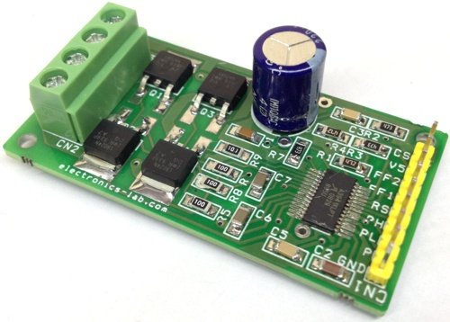
This tiny board designed to drive bidirectional DC brushed motor of large current. DC supply is up to 50V DC. A3941 gate driver IC and 4X N Channel Mosfet IRLR024 used as H-Bridge. The project can handle a load up to 10Amps. Screw terminals provided to connect load and load supply, 9 Pin header connector provided for easy interface with micro-controller. On board shunt resistor provides current feedback.

The A3941 is a full-bridge controller for use with external N-channel power MOSFETs and is specifically designed for automotive applications with high-power inductive loads, such as brush DC motors. A unique charge pump regulator provides full (>10 V) gate drive for battery voltages down to 7 V and allows the A3941 to operate with a reduced gate drive, down to 5.5 V. A bootstrap capacitor is used to provide the above-battery supply voltage required for N-channel MOSFETs. An internal charge pump for the high-side drive allows DC (100% duty cycle) operation.

The full bridge can be driven in fast or slow decay modes using diode or synchronous rectification. In the slow decay mode, current recirculation can be through the high-side or the low side FETs. The power FETs are protected from shoot-through by resistor R7 adjustable dead time. Integrated diagnostics provide indication of under voltage, over temperature, and power bridge faults, and can be configured to protect the power MOSFETs under most short circuit conditions.

The A3941 is a full-bridge MOSFET driver (pre-driver) requiring a single unregulated supply of 7 to 50 V. It includes an integrated 5 V logic supply regulator. The four high current gate drives are capable of driving a wide range of N-channel power MOSFETs, and are configured as two high-side drives and two low-side drives. The A3941 provides all the necessary circuits to ensure that the gate-source voltage of both high-side and low-side external FETs are above 10 V, at supply voltages down to 7 V. For extreme battery voltage drop conditions, correct functional operation is guaranteed at supply voltages down to 5.5 V, but with a reduced gate drive voltage. The A3941 can be driven with a single PWM input from a Microcontroller and can be configured for fast or slow decay. Fast decay can provide four-quadrant motor control, while slow decay is suitable for two-quadrant motor control or simple inductive loads. In slow decay, current recirculation can be through the high-side or the low-side MOSFETs. In either case, bridge efficiency can be enhanced by synchronous rectification. Cross conduction (shoot through) in the external bridge is avoided by an adjustable dead time. A low power sleep mode allows the A3941, the power bridge, and the load to remain connected to a vehicle battery supply without the need for an additional supply switch. The A3941 includes a number of protection features against under voltage, over temperature, and Power Bridge faults. Fault states enable responses by the device or by the external controller, depending on the fault condition and logic settings. Two fault flag outputs, FF1 and FF2, are provided to signal detected faults to an external controller.

Features

  • High current gate drive for N-channel MOSFET full bridge
  • High-side or low-side PWM switching
  • Charge pump for low supply voltage operation
  • Top-off charge pump for 100% PWM
  • Cross-conduction protection with adjustable dead time
  • 5 to 50 V supply voltage range
  • Integrated 5 V regulator
  • Diagnostics output
  • Low current sleep mode

Schematic

Parts List

Connections


Truth Table

Photos

RS485 Shield For Arduino Nano

Arduino Nano RS485 shield will help you to transmit and receive serial data using the twisted pair RS485 network. The module provides half-duplex communication. LED D1 indicates receive data, D2 Transmit LED, J1 jumper is optional and not in use in this application. DI/RE connected to D2 of Arduino digital pin which enables Receiver Output /Driver Output. CN1 connecter supply input, CN2 3 pin screw terminal helps to connected twisted pair cable.  The unit can communicate over 4000 feet of 26AWG twisted-pair wire at 110 kHz into 120Ω loads.

FEATURES

  • Supply 7-12V DC
  • D2 Transmit LED, D1 Receive LED
  • PCB Dimensions 40.46 x 17.98 mm

SCHEMATIC

PARTS LIST

PHOTOS


PCB

750mA Constant Current LED Driver Arduino Nano Shield


This small constant current LED driver Nano shield has been designed using CAT4104 IC from ON semiconductor. Its 4 channel LED driver. The board has provision to mount 20 SMD 1206 LEDs. The LED can be RED, GREEN, BLUE and WHITE. Reduce the number of LED to 12 if White LEDs are used, as white LEDs are 3-5V and total series voltage should not exceed 12V. CAT4104 provides four matched low dropout current sinks to drive high−brightness LED strings up to 175 mA per channel. The LED channel current is set by an external trimmer potentiometer connected to the RSET pin. The LED pins are compatible with high voltage up to 12V. The EN/PWM logic input supports the device enable and high-frequency external Pulse Width Modulation (PWM) dimming control. Thermal shutdown protection is incorporated in the device to disable the LED outputs whenever the die temperature exceeds 150°C. Nano LED shield can be used to develop intelligent lighting for Automotive and Architect since PWM pin of LED driver connected to D9 PWM pin of Arduino. The EN/PWM pin has two primary functions. One function enables and disables the device. The other function turns the LED channels on and off for PWM dimming control.

The device has a very fast turn−on time (from EN/PWM rising to LED on) and allows “instant on” when dimming LED using a PWM signal. Accurate linear dimming is compatible with PWM frequencies from 100 Hz to 5 kHz for PWM duty cycle down to 1%. PWM frequencies up to 50 kHz can be supported for duty cycles greater than 10%. PWM pin connected to D9 of Arduino.

Note: Replace D1, D6, D11, D16, D2, D7, D12, and D17 with 0 Ohms SMD 1206 Resistor in case of white LED used.

Features

  • Input supply 12V DC
  • LED Load 750mA (4 Channel)
  • Constant Current Adjustable with help of Trimmer Potentiometer
  • Thermal Protection Shutdown
  • PR2 Trimmer Pot Provided to Adjust the Constant Current 80mA to 750mA
  • D9/PWM Of Arduino Connected
  • PR1 Trimmer Pot Connected to A0 Pin of Arduino Nano for Dimming Application
  • PCB DIMENSIONS: 46.35 x 18.30 mm

Schematic

Parts List

Connections

Photos

PCB

ISOLATED CAN BUS TRANSCEIVER ARDUINO SHIELD

The module described here is an isolated CAN Transceiver module. This module can be used as a standalone module or as an Arduino Uno shield. A controller area network is a two-wire high-speed serial network typically used to provide data communication between host and nodes. The high-speed controller area network transceivers offer integrated isolation, high ESD and high fault protection. The project built using ISO1042 IC from Texas Instruments. The project requires 5V supply from the host side (Arduino) and separates 5V from the node side for isolation. The project supports up to 5Mbps data rate in CAN FD mode allowing much faster transfer of payload compared to classic CAN. D1 Power LED, CN1 Can bus communication, CN3 RJ45 CAN Communication.

The ISO1042 device is a galvanically-isolated controller area network (CAN) transceiver that meets the specifications of the ISO11898-2 (2016) standard. The ISO1042 device offers ±70-V DC bus fault protection and ±30-V common-mode voltage range. The device supports up to 5Mbps data rate in CAN FD mode allowing much faster transfer of payload compared to classic CAN. This device uses a silicon dioxide (SiO2) insulation barrier with a withstand voltage of 5000 VRMS and a working voltage of 1060 VRMS. Electromagnetic compatibility has been significantly enhanced to enable system-level ESD, EFT, surge, and emissions compliance. Used in conjunction with isolated power supplies, the device protects against high voltage and prevents noise currents from the bus from entering the local ground.

Note: Don’t populate TR1 CM choke. CM choke required when the device is used in a harsh EMC environment, it is 51uH 0.2A coupled inductor. J1 / J2 jumpers to be closed for normal operations.

FEATURES

  • Supply 5V DC Host (Arduino)-VC1
  • Supply 5V DC Node Side
  • Data Transfer Speed 5-Mbps

SCHEMATIC

PARTS LIST

CONNECTIONS

PHOTOS

PCB

+9V TO 60V PWM 2.3A SOLENOID VALVE DRIVER USING DRV101

The DRV101 is a low-side power switch employing a pulse-width modulated (PWM) output. Its rugged design is optimized for driving electromechanical devices such as valves, solenoids, relays, actuators, and positioners. The DRV101 module is also ideal for driving thermal devices such as heaters and lamps. PWM operation conserves power and reduces heat rise, resulting in higher reliability. In addition, an adjustable PWM potentiometer allows fine control of the power delivered to the load. The time from dc output to PWM output is externally adjustable. The DRV101 can be set to provide a strong initial closure, automatically switching to a soft hold mode for power savings. The duty cycle can be controlled by a potentiometer, analog voltage, or digital-to-analog converter for versatility. A flag output LED D2 indicates thermal shutdown and over/under the current limit. A wide supply range allows use with a variety of actuators.

FEATURES

  • HIGH OUTPUT DRIVE: 2.3A
  • WIDE SUPPLY RANGE: +9V to +60V
  • COMPLETE FUNCTION
  • PWM Output
  • Internal 24 kHz Oscillator
  • Digital Control Input
  • Adjustable Delay (Capacitor C1)
  • Adjustable Duty Cycle P1 Potentiometer
  • Over/Under Current Indicator
  • FULLY PROTECTED
  • Thermal Shutdown with Indicator
  • Internal Current Limit

APPLICATIONS

  • ELECTROMECHANICAL DRIVERS:
  • Solenoids Positioners
  • Actuators High Power Relays/Contactors
  • Valves Clutch/Brake
  • FLUID AND GAS FLOW SYSTEMS
  • INDUSTRIAL CONTROL
  • FACTORY AUTOMATION
  • PART HANDLERS
  • PHOTOGRAPHIC PROCESSING
  • ELECTRICAL HEATERS
  • MOTOR SPEED CONTROL
  • SOLENOID/COIL PROTECTORS
  • MEDICAL ANALYZERS

SCHEMATIC

PARTS LIST

PHOTOS

PCB

TYPE K THERMOCOUPLE SENSOR AMPLIFIER ARDUINO SHIELD

This is a Type K Thermocouple Sensor Amplifier Arduino Shield that enables an Arduino board to acquire temperatures from a thermocouple of type K. The shield works with a single supply and takes 5V DC from the Arduino board, the output of the circuit is 0 to 4V DC for 0-degree centigrade to 400C. The output of the amplifier is connected to the A0 analog pin of Arduino. A typical application of thermocouples is in boilers, soldering stations, and heaters. Also, 3D printers rely on thermocouples to measure the extruder temperature.

The K thermocouple has usually two wires, made of Alumel and Chromel that need to be connected with special care: no solder, just use a mechanical connection, therefore it is advisable to use special connectors available for thermocouples.

The circuit is built using LTC1049 op-amp and Thermocouple Cold Junction Compensator chip LTC1025. The board also supports other sensors like Type E, J, R, S, and T, however I have tested this circuit with Type K Sensor, jumpers are provided to use, and select other types of sensors.

The LTC1049 is a high performance, low power zero-drift operational amplifier. The two sample-and-hold capacitors usually required externally by other chopper stabilized amplifiers are integrated on the chip. Further, the LTC1049 offers superior DC and AC performance with a nominal supply current of only 200μA. The LTC1049 has a typical offset voltage of 2μV, drift of 0.02μV/°C, 0.1Hz to 10Hz input noise voltage of 3μVP-P and typical voltage gain of 160dB. The slew rate is 0.8V/μs with a gain-bandwidth product of 0.8MHz.

The LT®1025 is a micropower thermocouple cold junction compensator for use with type E, J, K, R, S, and T thermocouples. It utilizes wafer level and post-package trimming to achieve 0.5°C initial accuracy. Special curvature correction circuitry is used to match the “bow” found in all thermocouples so that accurate cold junction compensation is maintained over a wider temperature range. The LT1025 will operate with a supply voltage from 4V to 36V. The typical supply current is 80mA, resulting in less than 0.1°C internal temperature rise for supply voltages under 10V. A 10mV/°C output is available at low impedance, in addition to the direct thermocouple voltages of 60.9mV/°C (E), 51.7mV/°C (J), 40.3mV/°C (K, T) and 5.95mV/°C (R, S). All outputs are essentially independent of power supply voltage

FEATURES

  • Supply 5V DC
  • Thermocouple Sensor: Type K
  • Output 0 to 4V DC
  • Temperature Sensing range 0 to 400 Degree Centigrade
  • PCB dimensions: 31.75 x 51.12mm

SCHEMATIC

PARTS LIST

CONNECTIONS

GERBER VIEW

SAMPLE CODE

[sourcecode language=”C”]/*
AnalogReadSerial

Reads an analog input on pin 0, prints the result to the Serial Monitor.
Graphical representation is available using Serial Plotter (Tools > Serial Plotter menu).
Attach the center pin of a potentiometer to pin A0, and the outside pins to +5V and ground.

This example code is in the public domain.

http://www.arduino.cc/en/Tutorial/AnalogReadSerial
*/

// the setup routine runs once when you press reset:
void setup() {
// initialize serial communication at 9600 bits per second:
Serial.begin(9600);
}

// the loop routine runs over and over again forever:
void loop() {
// read the input on analog pin 0:
int sensorValue = analogRead(A0);
// print out the value you read:
Serial.println(sensorValue);
delay(1); // delay in between reads for stability
}[/sourcecode]

PHOTOS

VIDEO

PCB

HEAT ACTIVATED COOLING FAN CONTROLLER

Heat-activated cooling fan controller is a simple project which operates a brushless fan when the temperature in a particular area goes above a set point, when temperature return normal, fan automatically turns off. The project is built using LM358 Op-amp and LM35 temperature Sensor. Project requires 12V DC supply and can drive 12V Fan. This project is useful in application like Heat sink temperature controller, PC, heat sensitive equipment, Power supply, Audio Amplifiers, Battery chargers, Oven etc.  (more…)

SOUND SENSOR WITH ONBOARD RELAY ARDUINO NANO SHIELD

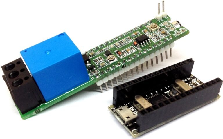
This sound sensor with Relay driver shield for Arduino Nano can be used to develop sound-activated ON/OFF switch or other projects that require sound senor. LM358 op-amp is used as the amplifier, 1st op-amp amplifies the microphone signal, and 2nd op-amp works as a half-bridge rectifier that converts AC signal into a DC voltage. This DC voltage is connected to analog pin A4 of Arduino Nano, further, this circuit has a comparator that provides High-level signal output and goes low as the sound is detected, this signal is connected to D4 Pin of Arduino Nano. The board provides a dual output, analog voltage as well as a digital output. The output of the sensor is normally high and goes low when it detects sound. PR1 Trimmer potentiometer is provided to set the threshold. PR2 Trimmer potentiometer can be used to set the sound sensitivity. On-Board 5V relay can be triggered using digital Pin D5 of Arduino Nano, Relay can drive a load up to 7Amps 12V DC or 230V AC. The circuit works with 5V DC and consumes approx. 50mA.

FEATURES

  • Supply 5V DC
  • Relay Switch Normally Open/ Normally Closed
  • Relay Switch 7Amps
  • DC Voltage Output Connected to A4 Analog Pin
  • Sensor Digital Output Connected to D4 Digital Pin
  • D5 Digital Pin Controls The Relay
  • PR2- Trimmer Potentiometer to set the sound sensitivity
  • PR1- Trimmer Potentiometer to set the threshold
  • CN1 Supply Input
  • CN4 Relay Output
  • PCB Dimensions 76.49 x 93 mm

SCHEMATIC

PARTS LIST

PHOTOS


PCB

2.7A PWM VALVE/SOLENOID DRIVER ARDUINO NANO SHIELD

This Arduino shield helps to drive various loads like a solenoid, valve, motor, inductive actuator, heater, and bulb. A wide supply range 8V-60V and a load current of 2.7A allows it to be used with a variety of actuators. The board can be used as a stand-alone driver or it can be controlled by Arduino Nano. DRV102 is the heart of the project which is a high-side power switch employing a pulse-width modulated (PWM) output. Its rugged design is optimized for driving electromechanical devices such as valves, solenoids, relays, actuators, and positioners. The circuit is also ideal for driving thermal devices such as heaters and lamps. PWM operation conserves power and reduces heat rise in the device, resulting in higher reliability. In addition, adjustable PWM allows fine control of the power delivered to the load. the delay from DC output to PWM output is externally adjustable using C1 capacitor.  The DRV102 can be set to provide a strong initial closure, automatically switching to a soft hold mode for power saving. The duty cycle can be controlled by resistor R3. LED D1 output indicates thermal shutdown and over/under current limit. D2 of the Arduino Nano connected to the input of DRV102 to control on/off of the load, J2 jumper can be used to on/off the load in stand-alone mode, J1 PCB jumper provided to run the project with a maximum signal supply of 9V. The project requires dual supply, Load supply 8-60V and logic supply 6-9V. (more…)

USBASP FIRMWARE UPDATE GUIDE

The USBASP programmer is an important tool/accessory for embedded systems engineers/ firmware developers. It is a USB ICSP (In-Circuit Serial Programmer) that allows developers to easily upload firmware/bootloaders on AVR microcontrollers. Unlike what you find to serial programmers like the USB-TTL converters, it does not use a dedicated chip as it runs on an atmega88 (or atmega8), and uses a firmware-only USB driver with no special USB controller required.

USBASP Programmer

While this firmware-only USB driver approach increases its compatibility, it also introduces a major challenge to the programmer as it requires regular updates for compatibility with advancements in how microcontrollers are programmed. One such advancement is the Tiny Programming Interface (TPI) that allows external programmers to access the nonvolatile memory (NVM) of certain low-end Atmel microcontrollers like the ATtiny series.

While features like TPI has been around for a while, using a USBASP programmer is still a problem as both old and new USBASP devices require a firmware update before they can be used. To help users who need this feature, today’s tutorial will spotlight the process involved in updating the firmware on your USBASP programmer to the latest version.

REQUIRED COMPONENTS

The following components are required to perform the firmware update:

  • The USBASP Programmer
  • An Arduino Uno (a nano should equally work)
  • Jumper wires
  • Breadboard

USBASP programmers, irrespective of brand, typically have the same configuration, so this tutorial should work, irrespective of the type or brand that you have.

PREPARE THE ARDUINO UNO

Uploading firmware to the USBASP requires a programmer. For today’s tutorial, we will use an Arduino Uno as that programmer. To make the Arduino a programmer, we need to upload a sketch, available among the examples on the Arduino IDE, to the Arduino board. Follow the steps below to do this:

  • Go to File > Examples > ArduinoISP
  • Connect an Arduino board to your PC
  • Select the port and board type and Click on Upload

With this done, the Arduino board is now ready to serve as a programmer.

SCHEMATICS

Next, we need to connect the USBASP to the Arduino Board. Using jumper wires and the breadboard (if necessary) connect the Arduino board and the USBASP device as shown in the image below:

Schematics

Since the fritzing model is not an exact replica of the popular USBASP types, a pin map showing how the Arduino is connected to the USBASP is provided below to make the connection easier to follow:

Arduino – USBASP

5v - VCC
GND - GND
D13 - SCK
D12 - MISO
D11 - MOSI
D10 - RESET

Go over the connections once again to ensure it’s properly done. If you have doubts about identifying the pins on your USBASP, you can run a google search for the pin-out of that particular board and use it as a guide for the connection.

With the boards connected, one more thing we need to do is to close the Jumper JP2 (highlighted below) on the USBASP board. Without doing this, we will not be able to upload firmware to the device. Close the jumper by bridging it with solder led or jumper wires.

With this done we are now ready to upload the firmware.

UPLOADING THE FIRMWARE

We start by downloading the firmware. A repository containing the latest version of the firmware is maintained on Thomas Fischl’s website. As at the time of this writing, the latest version which thankfully has TPI support was released in May 2011. Download that.

A key ingredient of the firmware upgrade process is the AVRDUDE. If you are familiar with the Arduino IDE, you would definitely have seen a reference to it in the verbose during code upload. The AVRDUDE is an utility to download, upload, and manipulate the ROM and EEPROM contents of AVR microcontrollers using the in-system programming technique (ISP). The easiest way to get the AVRDUDE is by fetching its executable located within your Arduino folder -> “ARDUINO FOLDER”/Java/hardware/tools/avr/bin/ or you can downloading it.

Once you have it, the next step is to find it’s configuration file; avrdude.conf file, which (if you follow the Arduino IDE route) would be at the directory -> “ARDUINO FOLDER”/Java/hardware/tools/avr/etc/

Put these two files (the AVRdude executable and configuration file) inside a folder along with the .hex file of the USBasp firmware we just downloaded. This helps shorten the length of the final command. With these done, connect the Arduino with the USBasp programmer attached to it, to your computer, and note down the port that was assigned to the Arduino by your computer.

Finally, open a terminal window, navigate inside the folder we created earlier, and run the command below:

./avrdude -C ./avrdude.conf -p m8 -c avrisp -P /dev/cu.usbmodem14101 -b 19200 -U flash:w:usbasp.atmega8.20110528.hex:i

Ensure you enter the right port after the option -P. If this succeeds without any error message, then your USBASP now has the latest firmware, and it’s ready for some action.

That’s it for this tutorial!

Do feel free to reach out to me via the comment section if you have any challenges with getting this to work.

References:

12V TO 24V @ 1A STEP-UP SWITCHING REGULATOR USING LM2585

This is a DC-DC step-up converter based on LM2585-ADJ regulator manufactured by Texas Instruments. This IC was chosen for its simplicity of use, requiring minimal external components and for its ability to control the output voltage by defining the feedback resistors (R1,R2). NPN switching/power transistor is integrated inside the regulator and is able to withstand 3A maximum current and 65V maximum voltage. The switching frequency is defined by the internal oscillator and it’s fixed at 100KHz.

LM2585_pinout
The power switch is a 3-A NPN device that can standoff 65 V. Protecting the power switch are current and thermal limiting circuits and an under-voltage lockout circuit. This IC contains a 100-kHz fixed-frequency internal oscillator that permits the use of small magnetics. Other features include soft start mode to reduce in-rush current during start-up, current mode control for improved rejection of input voltage, and output load transients and cycle-by-cycle current limiting. An output voltage tolerance of ±4%, within specified input voltages and output load conditions, is specified for the power supply system.

Schematic

Schematic

SPECIFICATIONS

  • Vin: 10-15V DC
  • Vout: 24V DC
  • Iout: 1A
  • Frequency: 100KHz

Schematic is a simple boost topology arrangement based on datasheet. Input capacitors and diode should be placed close enough to the regulator to minimize the inductance effects of PCB traces. IC1, L1, D1, C1,C2 and C5,C6 are the main parts used in voltage conversion. Capacitor C3 is a high-frequency bypass capacitor and should be placed as close to IC1 as possible.

All components are selected for their low loss characteristics. So capacitors selected have low ESR and inductor selected has low DC resistance.

At maximum output power, there is significant heat produced by IC1 and for that reason, we mounted it directly on the ground plane to achieve maximum heat dissipation.

PHOTOS

PARTS LIST

Part Value Package MPN Mouser No
C1 C2 33uF 25V 1Ω 6.3 x 5.4mm UWX1E330MCL1GB 647-UWX1E330MCL1
C3 0.1uF 50V 0Ω 1206 C1206C104J5RACTU 80-C1206C104J5R
C4 1uF 25V 1206 C1206C105K3RACTU 80-C1206C105K3R
C5 C6 220uF 35V 0.15Ω 10 x 10.2mm EEE-FC1V221P 667-EEE-FC1V221P
D1 0.45 V 3A 40V Schottky SMB B340LB-13-F 621-B340LB-F
IC1 LM2585S-ADJ TO-263 LM2585S-ADJ/NOPB 926-LM2585S-ADJ/NOPB
L1 120 uH 0.04Ω 30.5 x 25.4 x 22.1 mm PM2120-121K-RC 542-PM2120-121K-RC
R1 28 KΩ 1206 ERJ-8ENF2802V 667-ERJ-8ENF2802V
R2 R3 1.5 KΩ 1206 ERJ-8ENF1501V 667-ERJ-8ENF1501V
R4 1 KΩ 1206 RT1206FRE07931KL 603-RT1206FRE07931KL
LED1 RED LED 20mA 2.1V 0805 599-0120-007F 645-599-0120-007F

GERBER VIEW

SIMULATION

We’ve done a simulation of the LM2585 step-up DC-DC converter using the TI’s WEBENCH online software tools and some of the results are presented here.

The first graph is the open-loop BODE graph. In this graph, we see a plot of GAIN vs FREQUENCY in the range 1Hz – 1M and PHASE vs FREQUENCY in the same range. This plot is useful as it gives us a detailed view of the stability of the loop and thus the stability and performance of our DC-DC converter.

simulation_1

Bode plot of open control loop

What’s interesting on this plot is the “phase margin” and “gain margin“. The gain margin is the gain for -180deg phase shift and phase margin is the phase difference from 180deg for 0db gain as shown in the plot above. For the system to be considered stable there should be enough phase margin (>30deg) for 0db gain or when phase is -180deg the gain should be less than 0db.

On the plot above we see that the phase margin is ~90deg and that ensures that the DC-DC converter will be stable over the measured range.

The next simulation graph is the Input Transient plot over time.

simulation_2

Input Transient simulation

In this plot, we see how the output voltage is recovering when the input voltage is stepped from 10V to 15V. We see that 4ms after the input voltage is stepped the output has recovered to the normal output voltage of 24V.

The next graph is the Load Transient.

simulation_3

Load Transient simulation

Load transient is the response of output voltage to sudden changes of load or Iout. We see that the output current suddenly changes from 0,1A to 1A and that the output voltage drops down to 23,2V until it recovers in about 3ms. We also see that when the load is reduced from 1A to 0,1A, output voltage spikes up to ~25,5V, then rings until it recovers to 24V in about 4ms.

The last graph shows the Steady State operation of DC-DC converter @ 1A output.

simulation_4

This graph shows the simulated output voltage ripple and inductor current. We see that output voltage ripple is ~0,6Vpp and the inductor current has a peak current of 2,4A. The inductor we used is rated at max 5,6A DC so it can easily withstand such operating current and without much heating of the coil.

Operating point data (Vin=13V, Iout=1A)

Operating Values
Pulse Width Modulation (PWM) frequency Frequency 100 kHz
Continuous or Discontinuous Conduction mode Mode Cont
Total Output Power Pout 24.0 W
Vin operating point Vin Op 13.00 V
Iout operating point Iout Op 1.00 A
Operating Point at Vin= 13.00 V,1.00 A
Bode Plot Crossover Frequency, indication of bandwidth of supply Cross Freq 819 Hz
Steady State PWM Duty Cycle, range limits from 0 to 100 Duty Cycle 48.3 %
Steady State Efficiency Efficiency 93.2 %
IC Junction Temperature IC Tj 65.2 °C
IC Junction to Ambient Thermal Resistance IC ThetaJA 34.9 °C/W
Current Analysis
Input Capacitor RMS ripple current Cin IRMS 0.14 A
Output Capacitor RMS ripple current Cout IRMS 0.48 A
Peak Current in IC for Steady State Operating Point IC Ipk 2.2 A
ICs Maximum rated peak current IC Ipk Max 3.0 A
Average input current Iin Avg 2.0 A
Inductor ripple current, peak-to-peak value L Ipp 0.50 A
Power Dissipation Analysis
Input Capacitor Power Dissipation Cin Pd 0.01 W
Output Capacitor Power Dissipation Cout Pd 0.035 W
Diode Power Dissipation Diode Pd 0.45 W
IC Power Dissipation IC Pd 1.0 W
Inductor Power Dissipation L Pd 0.16 W

CONFIGURING OUTPUT VOLTAGE

The output voltage is configured by R1, R2 according to the following expression (Vref=1,23V)

VOUT = VREF (1 + R1/R2)

If R2 has a value between 1k and 5k we can use this expression to calculate R1:

R1 = R2 (VOUT/VREF − 1)

For better thermal response and stability it is suggested to use 1% metal film resistors.

MEASUREMENTS

measurements_1

measurements_2

LM2585-ADJ DATASHEET

PCB

8 channel inductive load driver Arduino shield

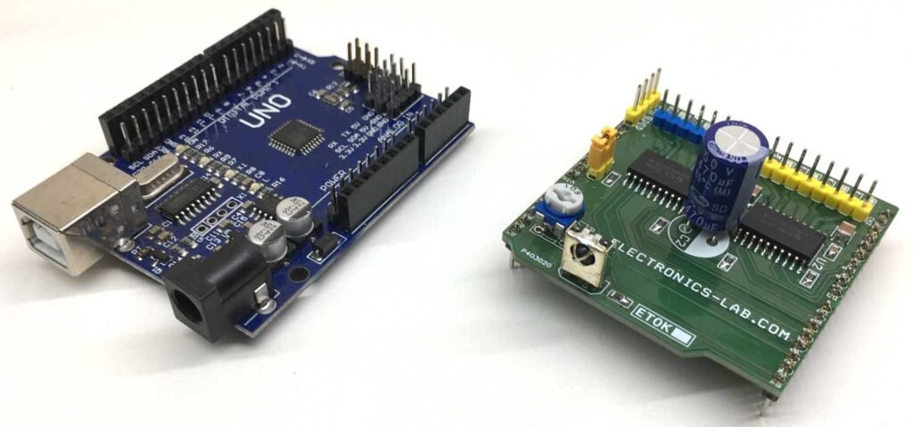
The 8 Channel Driver Arduino UNO Shield is designed to enable users to switch inductive loads for up to 800mA each channel and up to 24V DC with no heat-sink needed. It is ideal for such applications as driving 2x unipolar stepper motorssolenoids, relays, and small DC motors. It uses 2x DRV8803 Chip from Texas instruments which is 4 channel low side driver with over current protection. IC’s Internal shutdown protection function is provided for overcurrent protection, short circuit protection, under-voltage lockout, and over temperature. Faults are indicated by a fault output pin that is normally high and goes low if a fault condition occurs. Reset and enable pins has internal pull-down resistors. (more…)

12W Dimmer with soft start for 12V LEDs

The circuit presented here is a LED dimmer with a soft-start function. The board can drive a LED up to 12W and the circuit can manage a load up to 1A continuous with 12Vsupply. The circuit is built using SG3525 PWM IC and the IRFR120 MOSFET, SG3525 generates the PWM, and IRFR120 MOSFET drives the 12W max load. BC847 is used to invert the PWM signal from SG3525 and create a soft-start circuit. SG3525 has a soft-start function and the soft-start timing can be slowed down by increasing the capacitor C2 value to 22uF/16V.  Trimmer pot PR1 provided to adjust the PWM frequency from 210 Hz to 6.5Khz. Keeping PWM frequency lower is advisable for LED load. The intensity of the LED can be adjusted using the slider potentiometer P1. Optional small trimmer pot is provided in case slider pot is not available.  I have tried a LOG slider pot which is used in audio applications and a linear pot will have better linear dimming. The duty cycle upper limit can be restricted by changing R2. Use R2 0 Ohms or 1 Ohm for normal 0-100% duty output.

The circuit is designed to drive 12V LED or LED panels, so don’t connect directly any LED to this board, as LED forward voltage is 3.5V and they need a series resistor to control the current. Any LED, LED Panel, Light Pad of 12V, and current from 10mA to 1A can be connected to this board directly.

Direct drive of LED without a series resistor is possible by limiting the maximum current, choose the appropriate resistor value of R2 to achieve this.

FEATURES

  • Supply 12V-15V DC
  • LED Load 10mA to 1A continuous
  • Frequency range 210Hz to 6.5Khz
  • Duty Cycle Span 0 to 100 %
  • D1 Power LED

SCHEMATIC

PARTS LIST

CONNECTIONS

PHOTOS

GERBER VIEW

VIDEO

SG3525 DATASHEET

PCB

Optically isolated bidirectional I2C shield for Arduino

Optically isolator Arduino Shield has been designed to provide optically isolated I2C communication between Arduino and any other device or sensors that works with I2C protocols. I have used the ISO1540 Low-Power Bidirectional I2C Isolator IC from Texas Instruments to build this project, and the device is compatible with I2C interfaces. (more…)

Search for products

Back to Top
Product has been added to your cart